Analog Circuits
Physics and Basic Devices
Band Theory
Core Analogy:
A Band is just like a tube with water in. Water molecules here represent electrons, and bubbles represent holes.
Fermi-Dirac Distribution
The electrons are Fermions, which obey Fermi-Dirac Distribution:
$$
f(E)=\frac{1}{1+e^{(E-E_f)/kT}}
$$
Realize that $E_f$ is not a constant (change with temperature).
Band Diagram and Temperature
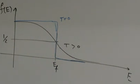
At 0K, the Fermi-Dirac distribution is exactly the step function. Corresponding to the analogy before, imagine two tubes holding parallel. The above one is empty and the tube below is full of water (The above band with higher energy than $E_f$ is empty, and the energy band lower than $E_f$ is full of electrons). Now everything stays still, no matter how hard you tilted the tubes, there’s no flow of water or bubbles, for all the particles are stuck in their own positions and all the positions are occupied.
As temperature arises, the diagram become smoother. Some electrons gain more energy than $E_f$ and some of them even overcome the restriction and become free. The positions below $E_f$ are released, i.e. producing holes, and some of the holes’ energy is so low that it could be regarded as free (really easy to transport because of the lower energy)
Calculate the n and p
An electron could be free if it’s energy is above $E_c$(constant), thus integrate $f(E)$ from $E_c$ to infinity is exactly what we want(Approximation should be applied to simplify the calculation):
$$
\int_{E_c}^\infty f(E)dE\approx \int_{E_c}^\infty \frac{1}{e^{(E-E_f)/kT}}dE \propto e^{(E_f-E_c)/kT}
$$
$$
\begin{equation}
n=N_c e^{(E_f-E_c)/kT}
\end{equation}
$$
For $p$, observe the diagram:
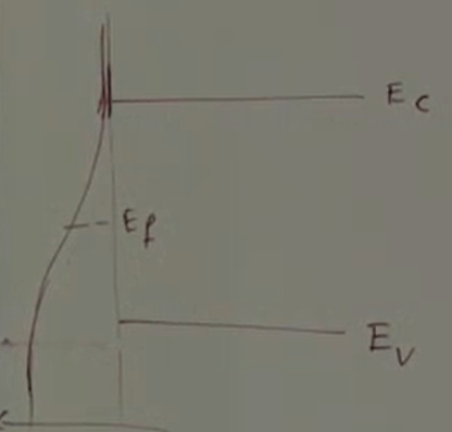
A hole could be free if any position of lower energy than $E_v$(constant) is released. The interval between $1$ and $f(E)$ is the probability of finding holes, thus integrate it:
$$
\int_{-\infty}^{E_v} (1-f(E))dE\approx \int_{-\infty}^{E_v} (1-(1-e^{(E-E_f)/kT}))dE \propto e^{(E_v-E_f)/kT}
$$
$$
\begin{equation}
p=N_v e^{(E_v-E_f)/kT}
\end{equation}
$$
Analysis
Note that intrinsic semiconductors have equal amount of $p$ and $n$. So we write it as $n_i$ and the $E_f$ now is denoted by $E_i$. Combining the formulas above:
$$
n_i=N_c e^{(E_i-E_c)/kT}=N_v e^{(E_v-E_i)/kT}\propto e^{(E_v-E_c)/kT}
$$
where the $E_v-E_c$ is the width of the band gap. We successfully throw $E_f$ away! And get the constant $n_i$.
Hence we derive:
$$
n=n_i e^{\frac{E_f-E_i}{kT}}
\qquad
p=n_i e^{\frac{E_i-E_f}{kT}}
$$
and the equation below holds:
$$
np=n_i^2
$$
So far we only analyzed the distribution caused by thermal equilibrium.
Diffusion current
The **net current** of holes is given by: $$ J_p(x)=-qD_p\nabla p(x) $$The net current of electrons is given by:
$$
J_n(x)=qD_n\nabla n(x)
$$
PN Junction
Initial equilibrium state
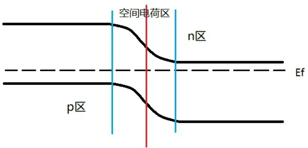
Observe the diagram below:
Explain:
At a given temperature and given conditions,$E_f$ is a constant inside the whole PN-Junction. (can be proved)
We denote p-type part’s $E_c$ energy as $E_{cp}$, n-type part’s energy as $E_{cn}$ etc. Analyze electron’s concentration now.
left part:
$$
n_p=N_c e^{(E_f-E_{cp})/kT}\approx \frac{n_i^2}{N_A}
$$
(remember $n_i$ is an eigen-value, independent of the dopants, thus remain constant in the whole material)
right part:
$$
n_n=N_c e^{\frac{E_f-E_{cn}}{kT}}\approx N_D
$$
where $N_A$ and $N_D$ represents the density of Acceptor and Donor respectively. Because we think the donor and acceptor ionize almost completely, $N_A$ is the density of holes at the left part and the $N_D$ is the density of electrons at the right part. Say $N_A=N_v e^{(E_{vp}-E_f)/kT}$ and $N_D=N_c e^{(E_f-E_{cn})/kT}$.[see Equation (1) and (2)]
so that
$$
\frac{n_p}{n_n}=\exp^{\frac{E_{cn}-E_{cp}}{kT}}\approx \frac{n_i^2}{N_A N_D}
$$
The depletion region exerts an electric field which tilted the electron energy diagram, at the left area, electrons potential shifted upward and the right part downward. $E_v$ approaches $E_f$ in p-type semiconductor and $E_c$ approaches $E_f$ in n-type semiconductor.
By the way, we may relate the parameters above to the potential change: $q \Delta \psi=E_{cn}-E_{cp}$, Therefore:
$$
\Delta\psi=\frac{kT}{q}\ln(\frac{N_A N_D}{n_i^2})
$$
Forward-Biasing electric field
Extra source producing forward-biasing electric field: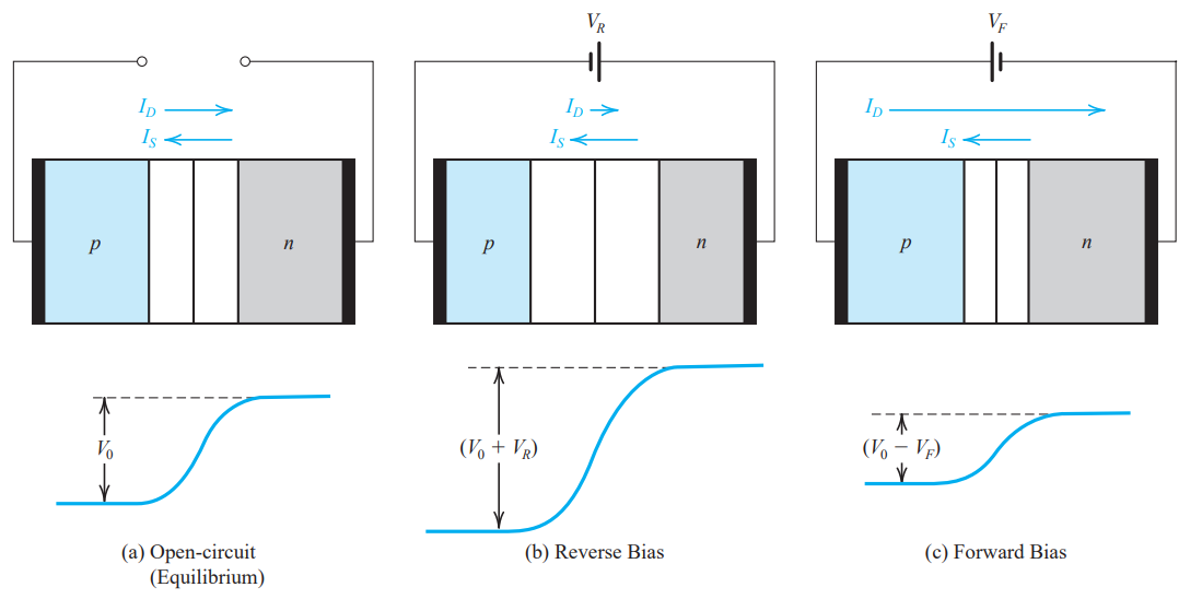
Understand the process intuitively:
The extra electric field produced by the source shifted the whole diagram, the electrons’ potential at left is lowered, which allows more electrons at right be able to traverse through the barrier.
Now calculate it according to our intuition:
At p-junction part, the electron’s potential was $-q\psi_0$ initially, and decreased to $-q(\psi_0-V_D)$.
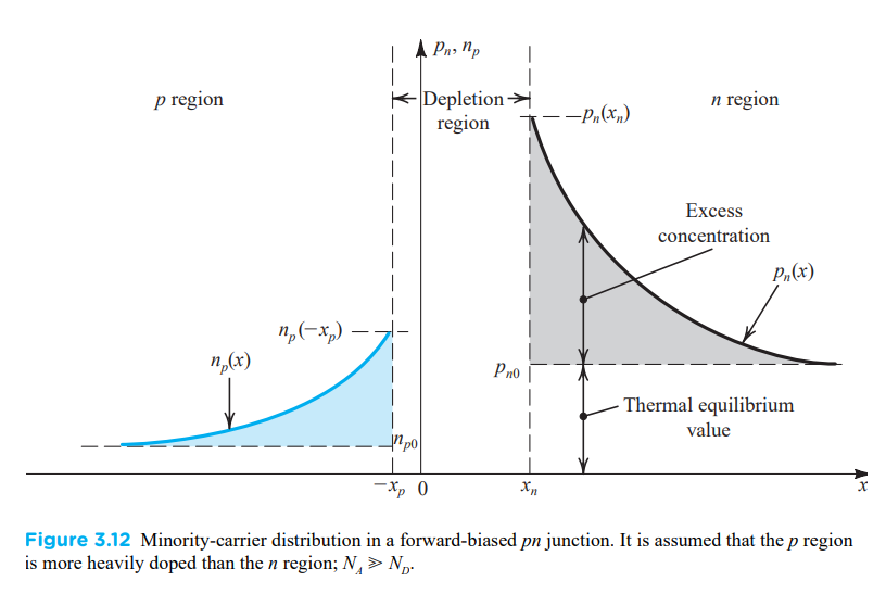
Remember that the concentration of the electron of qualified energy is proportional to the $e^{-q(\text{potential})/kT}$. The forward-bias voltage $V_D$ results in an excess concentration of electrons at the edge of depletion region and p-region. The current is proportional to that (why?):
$$
J_n\propto (e^{\frac{-q(\psi_0-V_D)}{kT}}-e^{\frac{-q(\psi_0)}{kT}})=e^{\frac{-q(\psi_0)}{kT}}(e^{\frac{qV_D}{kT}}-1)
$$
Or more compact:
$$
I=I_s(e^{\frac{qV_D}{kT}}-1)
$$
Be more specific about “why”
$\mathtt{Q}1$: Why is the situation with an extra electric field could provide current while the initial thermal equilibrium could not?$\mathtt{A}1$:In the thermal equilibrium case, the diffusion equals to the backward propagation caused by interior electric field. In the latter case, the diffusion tendency remains the same, while the barrier is much easier to overcome, thus the current is in fact the out-weight section of diffusion.
$\mathtt{Q}2$: Why is the current proportional to the excess concentration?
$\mathtt{A}2$: Note that $e^{\frac{-q(\psi_0)}{kT}}$ is the amount of electrons could pass through the depletion barrier before, and $e^{\frac{-q(\psi_0-V_D)}{kT}}$ is the amount of carriers could travel across the depletion region now. Then review This and Read Microelectronic Circuits Section 3.5.2
Capacitance
Bipolar Transistor
current flow
It can be shown that the minority-carrier concentration $n_p(x)$ in the base varies linearly with distance.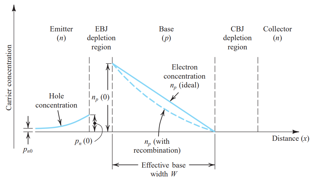
The gradient of $n_p(x)$ is the flow, an important observation here is that the current in collector region is the flow here, because the electric field guard the electrons to traverse to the collector, hence (expression of $n_p(0)$ was already shown in pn junction part):
$$
I_C=\text{flow in Base}\propto \frac{n_p(0)-0}{W}=\frac{e^{\frac{-q(\psi_0-V_D)}{kT}}}{W}\propto \frac{e^\frac{qV_D}{kT}}{W}
$$
denote $V_T=\frac{q}{kT}$ and pack constant into $I_s$, and $V_D$ is $V_{BE}$.
$$
I_C=I_s e^{V_{BE}/V_T}
$$
The $I_c$ is independent of $V_{CB}$, and only decided by $V_{BE}$.
Key modification
$\mathtt{Q}$: What’s then key factor that cause BJT’s privilege over a diode?
$\mathtt{A}$: Key point is the concentration profile change in n-region:
At the diode case, the concentration profile at n-region is an exponentially decreasing curve, reaching thermal equilibrium density at the end; while the BJT case the concentration profile is a sharp linear line, reaching zero at the end.
The latter case obviously provide larger current than the previuos one.
Base current
The recombination ratio is nearly constant. In other words, the number of electrons lost in recombination is proportional to the density ($e^{V_{BE}/kT}$), the more electrons come, the more holes would be combined, which is natural to admit.
After the recombination, base lost certain holes, and as a responding, the external circuit injects some to maintain it. So the extra current $I_B$ is proportional to the rate of losing holes, i.e. $\propto$ recombination ratio $\propto$ density.
$\mathtt{Q}$:Why is recombination happening?
$\mathtt{A}$:Because the holes aren’t fixed, some will drift to the emitter, and the drifting rate is also proportional to the density.
In conclusion, $I_B$ is proportional to the density
$$
I_B\propto e^{V_{BE}/V_T}
$$
as from the above section:
$$
I_C\propto e^{V_{BE}/V_T}
$$
The $I_C$ and $I_B$ could be linked by a coefficient $\beta$.
Proof of the Density Profile
The common case with **recombination**. Firstly we suppose naturally: $$ \text{flow}=-\nabla n $$ $\Delta\text{flow}$ of a segment $\Delta x$ is equal to the recombination rate (RHS) $\propto $ the volume of the segment and the density of the carriers, i.e. $$ (-\frac{\partial n}{\partial x} \left.\right\vert_x)-(-\frac{\partial n}{\partial x}\left.\right\vert_{x+\Delta x})=k\Delta x n $$ where k>0. Thus: $$ \frac{\partial^2 n}{\partial x^2}-kn=0 $$ This ode is quite easy to solve, with the form of exponential term: $$ n=C_1 e^{\sqrt{k}x}+C_2 e^{-\sqrt{k}x} $$ considering the _Boundary Condition_, easy to throw the first term out and derive the **exponentially decreasing profile**.What if there’s no recombination at all?
The RHS$=0$ which implies:
$$
\frac{\partial^2 n}{\partial x^2}=0
$$
The solution is simple:
$$
n=kx+b
$$
which is precisely the linear profile.
Engineering models
Operational Amplifier
differential-input, single-ended-output
An ideal Op Amp has infinite input impedance, because the input current is zero, which is the denominator in the definition of input impedance.
Its output impedance is zero, because the output voltage is $A(v_2-v_1)$, and no matter how large the load resistance is (i.e. no matter how large the current is), the output voltage won’t change as long as the input remains. This means that the impedance has to be zero.
Also the common mode rejection ($K_{CMR}$) is infinite.
An important characteristic of op amps is that they are direct-coupled or dc amplifiers.
The ideal op amp should have a gain A whose value is very large and ideally infinite.
One may justifiably ask: If the gain A is infinite, how are we going to use the op amp?
The answer is very simple: In almost all applications the op amp will not be used alone in a so-called open-loop configuration.
Rather, we will use other components to apply feedback to close the loop around the op amp.
The bandwidth shall be regarded as infinite too.
virtual short circuit
If we assume that the circuit is working and producing a finite output voltage at terminal 3, then the voltage between the op-amp input terminals should be negligibly small and ideally zero.
$$v_2-v_1=\frac{v_o}{A}=0
$$
We speak of this as the two input terminals “tracking each other in potential.”
Use the closed-loop method, we are trading gain for accuracy!
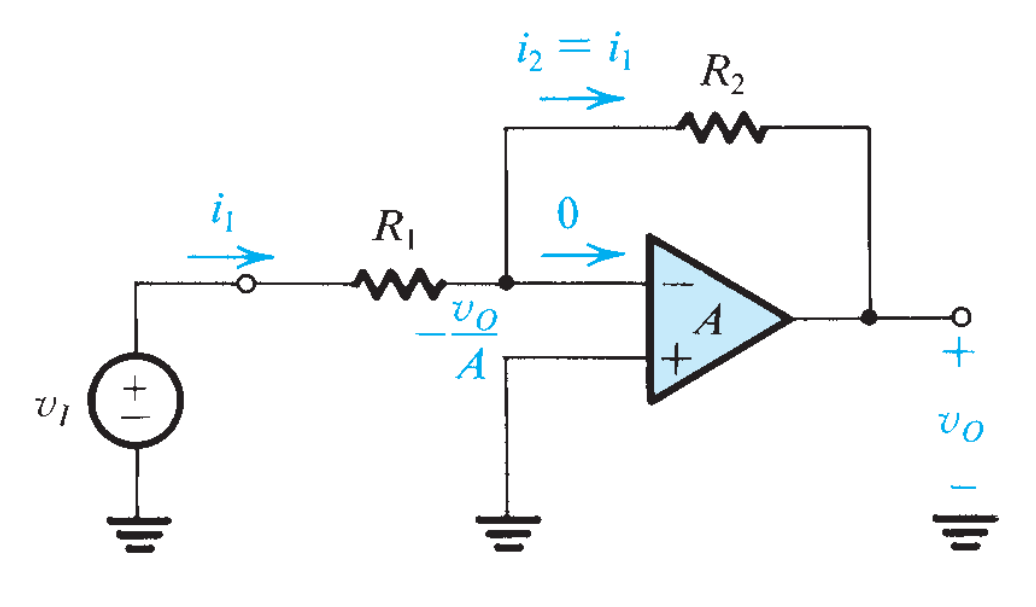
Also we may derive like this: suppose the gain is finite $A$ first, and as $v_{(+)}-v_{(-)}=\frac{v_o}{A}$, which is $v_{(-)}=-\frac{v_o}{A}$.
and the current shall be $iR_1=v_I-v_{(-)}$, and $iR2=v_{(-)}-v_o$, hence the final gain is:
$$
A_f=\frac{v_o}{v_I}=\frac{-R_2/R_1}{1+(1+R_2/R_1)/A}\to -\frac{R_2}{R_1}
$$
Besides the input resistance shall be $R_1$, as by definition: $\frac{V_I-0}{i}=R_1$. The output resistance remains zero still, because the output voltage is irrelevant to the output current.
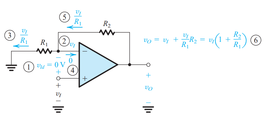
for this the analysis yields $A_f=1+\frac{R_2}{R_1}$. Besides the input resistance is infinite, as no current flows in. The output resistance is zero still, by the same reason as above.


